Categories
{{ selectedCategory.name }}
Infineon TriCore: Failed to initialize debug session / DAP Initialization failed
Possible causes:
- Faulty hardware: Target, Debug Adapter or Active Probe
- CPU is always in reset or debugger cannot reset the CPU
- Bad contact if the CPU is in a socket
- External watchdog resets the chip periodically
- DAP Wide mode is selected in Hardware / CPU Options / SoC, however, only DAP Standard mode is supported by the CPU
- DAP Standard / Wide is selected, but the JTAG Debug channel is configured via TRST' pin
Possible solutions
Change the hardware
- Try with another Target if available.
- If you are using a custom board, use an evaluation board from Infineon and winIDEA Example Workspaces.
- Try with another Debug Adapter or Active Probe
Verify, if a signal PORST’ is always low
The reason could be:
- Faulty target or Debug Adapter (refer to the first solution) or
- Active watchdog which holds the signal to logic low level.
You should:
- Detect and log reset on PORST’ pin. Refer to the topic Active Watchdog issues (solution logging).
- Use Logic Analyzer (if available) and verify, if the DAP that starts the sequence, corresponds to the sequence shown in the example below.
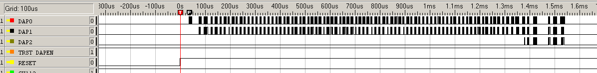
The start of emulation on TriCore DAP. Trigger is set to the positive edge on RESET. After reset DAP communication goes via two lines (DAP0 and DAP1). It switches to 3 pin mode if DAP Wide is selected. DAP protocol is a message based protocol. Debugger sends command (telegram) and ECU answers to command at the same line.
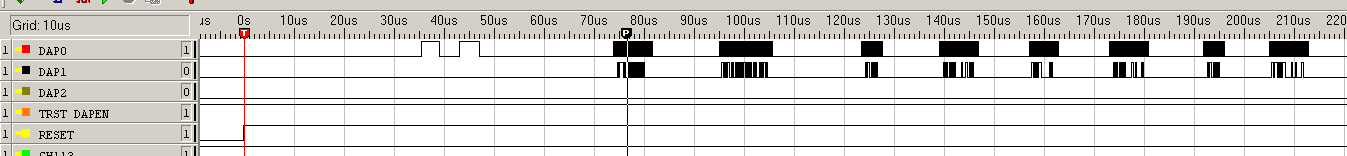
Zoomed recording when reset is released.
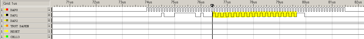
Zoomed recording when first DAP telegram is sent. First telegram is SYNC telegram where ECU answer with 0xAAAAAAAA (See the 10101010101010101 stream).
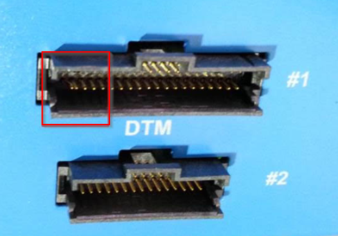
Bent pin on the BlueBox connector
(In most cases that is the pin 40 on ST1 connector). Bent pin disables connection between the debugger and the Target or causes a short-circuit with the pin 38 which is usually most of the time low.
Bad contact between CPU and the socket
- Power off the Target and the debugger.
- Carefully press the socket down a few times to realign the CPU.
- Carefully remove the CPU from the socket and clean both the CPU and the socket before you insert the CPU back.
Disable watchdogs
winIDEA uses a FLASH monitor which is used to program FLASH during download operation. The debugger first initializes part of the target RAM where the monitor will be placed, then downloads the monitor and execute it. If an external watchdog is triggered it causes the CPU to reset which invalidates RAM and the flash monitor stops working hence error message displayed by the debugger. Refer to the topic Active Watchdog issues.
Refer to the Infineon’s documentation
Check which Debug Mode (Standard, Wide) is supported.
Make sure that selection in winIDEA (Hardware / CPU Options / SoC) corresponds with the actual logic levels on TRST’ pin during power on reset.
It is recommended to connect the TRST' pin:
- via pull-up resistor to the VCC and to the DAP connector or
- via pull-down resistor to the GND and to the DAP connector
Signal TRST’ (previously DAPEN) is used to select either DAP or JTAG on power on reset. It is important which logic level is present on the TRST' pin during power on reset sequence: if logic 0 - JTAG is selected; if logic 1 - DAP is selected.
Sorry this article didn't answer your question, we'd love to hear how we can improve it.
Note: This form won't submit a case. We'll just use it to make this article better.
Similar topics
{{ topic.Title }} {{ topic.Ddate | formatDate }}
{{ topic.Content }}