Categories
{{ selectedCategory.name }}
Infineon Aurix TC3xx: Programming DFLASH1 when configured as HSM exclusive memory
By default, Data Flash (DFLASH), which is divided into two banks DFLASH0 and DFLASH1, is programmed through the regular debug download (fast flash programming based on flash programming monitor) via Hardware / Infineon <device> / Configure.
DFLASH can be split and used separately by the user application and the security application. When DFLASH1 is configured as the HSM exclusive memory (in the UCB), it cannot be programmed through the regular debug download under the above configuration. In this case, DFLASH1 can be programmed only either by the HSM or via a debug interface, a so-called Cerberus. Programming through the Cerberus is noticeably slower comparing to programming through the regular debug download.
Solution
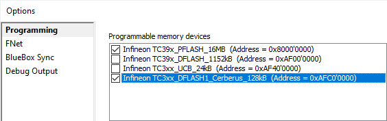
1. Open Hardware / Options / Programming.
2. Uncheck the DFLASH device at address 0XAF00’0000 in Programmable memory devices section.
3. Check the DFLASH1_Cerberus device at the end of the list. In this case, the debugger will program this memory region via the Cerberus.
When DFLASH1 is not configured as the HSM exclusive memory, program this memory area through the default DFLASH device selected (in Hardware / Options / Programming check DFLASH device). In principle, it could be also programmed via the Cerberus, but the programming is much slower and the other DFLASH0 bank cannot be programmed via the Cerberus.
Sorry this article didn't answer your question, we'd love to hear how we can improve it.
Note: This form won't submit a case. We'll just use it to make this article better.
Similar topics
{{ topic.Title }} {{ topic.Ddate | formatDate }}
{{ topic.Content }}